Tampilkan postingan dengan label Control. Tampilkan semua postingan

Minggu, 22 April 2012

Rangkaian Pengendali Motor DC model Darlington

Kumpulan Skema Elektronika, A normal variable resistor cannot directly control the speed of a motor since motors draw large amounts of current which would burn out the potentiometer. Instead, the small amount of current that the potentiometer can pass can be amplified into order to run the motor. This amplification can be achieved using Darlington Pair of transistors.

Rangkaian Pengendali Motor DC
Pin-out BFY61 & TIP31C Transistor

The circuit above shows a linear potentiometer connected Between Vs and 0V Such That the voltage at its wiper terminal will of always be somewhere at or Between these two voltages. The small amount of current flowing out of the potentiometer's wiper is amplified by two transistors, connected together in a configuration known as a 'Darlington pair'. The current from the potentiometer is amplified by the first transistor, and then again by the second transistor, greatly Increasing the amount of current That cans be controlled by the potentiometer.

There are, however, a couple of disadvantages of this simple circuit. Firstly, about 0.7V is lost in EACH of the transistor, so the maximum voltage cans That ever be applied to the motor is Vs - 1.4V. Secondly, the transistors are not absolutely linear so the change in motor speed for a given rotation of the potentiometer will from some more subtle in the middle of its range. Because a motor is an inductive load, it will from Produce a 'back-emf' Could the which damage to the second transistor. The 1N4148 signal diode prevents this damage by shorting out the back-emf.

The power supply for this circuit should preferably be un-smoothed (i.e. directly from the power supply rectifier). This helps prevent the motor 'sticking' at low speeds. With the TIP31C transistor given, the maximum power supply voltage may be 60V and the maximum motor current consumption may be 3A.

Source: www.eleinmec.com

Sabtu, 21 April 2012

Rangkaian Timer On-Off 24 Jam

Timer On-off 24 Jam. This is a circuits are multi-range timers offering periods of up to 24 hours and beyond. This circuit can be used as repeating timers - or as single-shot timers

Skema Rangkaian On/Off 24 Hours Timer

The Cmos 4060 is a 14-bit binary counter. However - only ten of those bits are connected to output pins. The 4060 also has two inverters - connected in series across pins 11, 10 & 9. Together with R3, R4, R5 and C3 - they form a simple oscillator.

While the oscillator is running - the 14-bit counter counts the number of oscillations - and the state of the count is reflected in the output pins. By adjusting R4 you can alter the frequency of the oscillator. So you can control the speed at which the count progresses. In other words - you can decide how long it will take for any given output pin to go high.

When that pin goes high - it switches the transistor - and the transistor in turn operates the relay. In single-shot mode - the output pin does a second job. It uses D1 to disable the oscillator - so the count stops with the output pin high.

If you want to use the timer in repeating mode - simply leave out D1. The count will carry on indefinitely. And the output pin will continue to switch the transistor on and off - at the same regular time intervals.

Note:
  • Using "Trial and Error" to set a long time period would be very tedious. A better solution is to use the Setup tables provided - and calculate the time required for Pin 7 to go high. For example, if you want a period of 9 Hours - the Range table shows that you can use the output at Pin 2. You need Pin 2 to go high after 9 x 60 x 60 = 32 400 seconds. The Setup table tells you to divide this by 512 - giving about 63 seconds. Adjust R4 so that the Yellow LED lights 63 seconds after power is applied. This will give an output at Pin 2 after about 9 Hours.
  • Ideally C3 should be non-polarized - but a regular electrolytic will work - provided it doesn't leak too badly in the reverse direction. Alternatively - you can simulate a non-polarized 10uF capacitor by connecting two 22uF capacitors back to back
  • The timers were designed for a 12-volt supply. However - provided a suitable relay is used - both circuits will work at anything from 5 to 15-volts. Applying power starts the timer. And it can be reset at any time by a brief interruption of the power supply.
Sorcer: http://www.zen22142.zen.co.uk/

Sabtu, 31 Maret 2012

Rangkaian Kontrol Kecepatan Wiper Mobil

For some car wiper speed sometimes just made some speed so that less appropriate when we want a different speed, but for those of you who want a digital wiper speed controller you can also use this circuit to replace your old system.

rangkaian kontrol kecepatan wiper mobilSkema rangkaian kontrol kecepatan wiper mobil

This circuit comprises 2 timer NE555 ICs, one CD4017 decade counter, one TIP32 driver transistor, a 2N3055/ TIP3055 power transistor and A Few other discrete components. Timer IC1 is configured as a mono-stable multivibrator produces a pulse Pls Which one presses switch S1 momentarily. This pulse acts as a clock pulse for the decade counter (IC2) Which advances by one count on Each successive clock pulse or the push of switch S1. Ten presets (VR1 through VR10), for Different sets of values by trial and error, Are Used At The ten outputs of IC2. But since only one output of IC2 is high at a time, only one preset (selected at the output) effectively comes in series with resistors R4 and R5 timing connected in the circuit of timer IC3 Which functions in astable mode. As presets VR1 through VR10 are set for Different values, Different time periods (or frequencies) for astable multivibrator IC3 Can be selected. The output of IC3 is applied to the pnp driver transistor TIP32 for driving the final power transistor 2N3055 Which in turn drives the wiper motor at the selected sweep speed. The power supply for the wiper motor as well as the circuit is tapped from the vehicle s battery Itself. The duration of the monostable multivibrator IC1 is set for a period of nearly one second.

Source : www.electronic-circuits-diagrams.com

Touch volume control circuit

Touch controls are not only used to switch devices on or off. They can also be used to control different functions. One good example is the TV remote control. If it is very important to keep the activated functions for a long period of time, it is always better to use a digital memory system. However, if small drifts in the control status is acceptable, a simple analog design can be used to memorize the status.


The touch volume controller is one such analog memory touch control switch. The main function centers mostly on the IC1. It is an opamp configured as an integrator with a high impedance input. If sensor 1 is touched, the capacitor C2 charges through the skin resistance and voltage at the output of IC1 decreases linearly until it reaches zero volt. Touching the other sensor (sensor 2) will produce the opposite result: the voltage at the pin 6 of IC1 will increase linearly until it reaches the power supply level. The special function of this touch volume control circuit is that after moving your finger away from the sensor(s), the output voltage of IC1 stays at that level.
This voltage value is memorized by C2. This analog memory however has a problem in long time periods: The voltage value drifts away by 2 % per hour due to the unavoidable current leak in the capacitor. To improve this situation, it is highly recommended to put this circuit in a moisture proof box.
This touch volume controller circuit has a wide application range. It can be used in devices where a potentiometer can be controlled through voltage levels. The touch sensors can alse be replaced with conventional push button switches. The capactiors C1 and C4 are very important in the circuit: they prevent the IC1 from oscillating. Simultaneously closing both switches will not damage the circuit.

Touch volume control PCB layout


Rabu, 28 Maret 2012

Brightness Controller Circuit For Small Lamps and Leds


Circuit diagram:

Brightness Controller Circuit For Small Lamps and Leds


This device was designed on request; to control the light intensity of four filament lamps (i.e. a ring illuminator) powered by two AA or AAA batteries, for close-up pictures with a digital camera. Obviously it can be used in other ways, at anyone’s will.IC1 generates a 150Hz square wave having a variable duty-cycle. When the cursor of P1 is fully rotated towards D1, the output positive pulses appearing at pin 3 of IC1 are very narrow.
Bulb LP1, driven by Q1, is off as the voltage across its leads is too low. When the cursor of P1 is rotated towards R2, the output pulses increase in width, reaching their maximum amplitude when the potentiometer is rotated fully clockwise. In this way the bulb reaches its full brightness.

 Parts:
P1 = 470K
R1 = 10K
R2 = 47K
R3 = 1.5K
C1 = 22nF-63V
C2 = 100uF-25V
D1 = 1N4148
D2 = 1N4148
Q1 = BD681
B1 = 2xAA cells in series
IC1 = 7555 or TS555CN
LP1 = 1.5V 200mA Bulb
SW1 = SPST Switch

Notes:
  • LP1 can be one or more 1.5V bulbs wired in parallel. Maximum total output current allowed is about 1A.
  • R2 limits the output voltage, measured across LP1 leads, to 1.5V. Its actual value is dependent on the total current drawn by the bulb(s) and should be set at full load in order to obtain about 1.5V across the bulb(s) leads when P1 is rotated fully clockwise.

Senin, 26 Maret 2012

Ultrasonic Remote Control (Rangkaian Remot kontrol Ultrasonic)

This is a remote control circuit employing ultrasonic signals. The ultrasonic transmitter circuit is build around IC1(NE 555). IC1 is an astable multi vibrator operating at 40KHz.The output of IC1 is amplifier the complementary pair of transistors ( Q1 & Q2) and transmitted by the ultrasonic transmitter K1. The switch S1 is used activate the transmitter.

remote ultrasonicSkema rangkaian remote Control ultrasonic

Note:
  • switch S1 can be a push button switch.
  • The preset R16 can be used to adjust the sensitivity of the receiver.
  • The frequency of the ultrasonic signal can be varied by adjusting the preset R17.Adjust it for optimum performance.


The ultrasonic receiver uses an sensor transducer (K2) to sense the ultrasonic signals. When an ultrasonic signal is falling on the sensor, it produces a proportional voltage signal at its output. This weak signal is amplified by the two stage amplifier circuit comprising of transistors Q3 and Q4.The output of the amplifier is rectified by the diodes D3 & D4.The rectified signal is given to the inverting input of the opamp which is wired as a comparator. When ever there is an ultrasonic signal falling on the receiver, the output of the comparator activates the transistors Q5 & Q6 to drive the relay. In this way the load connected via the relay can be switched. The diode D5 is used as a free wheeling diode.


Features IC CA3140


  • Very High Input Impedance (ZIN) -1.5TΩ (Typ)
  • Very Low Input Current (Il) -10pA (Typ) at ±15V
  • Wide Common Mode Input Voltage Range (VlCR) - Can be wung 0.5V Below Negative Supply Voltage Rail
  • Output Swing Complements Input Common Mode
  • Directly Replaces Industry Type 741 in Most Applications
  • Pb-Free Plus Anneal Available (RoHS Compliant)


Pin Connection Ic NE 555


  • Ground, is the input pin of the source of the negative DC voltage
  • Trigger, negative input from the lower comparators (comparator B) that maintain oscillation capacitor voltage in the lowest 1 / 3 Vcc and set RS flip-flop
  • Output, the output pin of the IC 555.
  • Reset, the pin that serves to reset the latch inside the IC to be influential to reset the IC work. This pin is connected to a PNP-type transistor gate, so the transistor will be active if given a logic low. Normally this pin is connected directly to Vcc to prevent reset
  • Control voltage, this pin serves to regulate the stability of the reference voltage negative input (comparator A). This pin can be left hanging, but to ensure the stability of the reference comparator A, usually associated with a capacitor of about 10nF to berorde pin groun
  • Threshold, this pin is connected to the positive input (comparator A) which will reset the RS flip-flop when the voltage on the capacitor from exceeding 2 / 3 Vc
  • Discharge, this pin is connected to an open collector transistor Q1 is connected to ground emitternya. Switching transistor serves to clamp the corresponding node to ground on the timing of certain
  • Vcc, pin it to receive a DC voltage supply. Usually will work optimally if given a 5-15V. the current supply can be seen in the datasheet, which is about 10-15mA.

Jumat, 23 Maret 2012

Rangkaian Lampu mati nyala Otomatis

Rangkaian Lampu Halaman Belakang. Sebagai bagian dari bangun rumah, halaman belakang biasanya ada. Beragam fungsi serta peran yang dimainkannya. Halaman belakang, menjelma menjadi taman-taman indah nan artistik, penuh sentuhan nilai seni pada rumah yang mewah. Tak jarang, kolam renang dengan air kebiruan menjadi pelengkapnya. Di lain pihak, halaman belakang adalah tempat menimbun perkakas yang tidak penting dari suatu
rumah sederhana yang kelebihan perabot.
Tempat bercengkerama keluarga, menyatukan pendapat, berbagi cerita dan cinta. Wahana menikmati secangkir teh, susu atau kopi panas di pagi hari sambil membaca koran. Di sore hari, halaman belakang bisa menjadi tempat pelepas lelah dan penat setelah seharian bekerja. Kursi malas dengan busa empuk, meja-meja bundar bercita rasa seni, tumpukan koran dan buku, beberapa toples cemilan akan lengkap dinikmati di halaman belakang.
Pada kesempatan kali ini saya akan mengetengahkan dan memperkenalkan sebuah rangkaian, yakni Rangkaian Lampu Halaman Belakang.

Rangkaian ini akan bekerja/berfungsi dari pukul 10 malam sampai pagi. Hal ini membantu untuk memberikan cahaya di halaman belakang guna menghindari binatang malam dan bahkan mencegah upaya pencurian. Rangkaian ini sepenuhnya otomatis dan menggunakan LDR sebagai saklar peka cahaya.
Rangkaian memiliki power supply tanpa trafo  dan rangkaian saklar berbasis waktu. Kapasitor C1, dioda D1 dan kapasitor C2 melalui D4 membentuk bagian power supply. C1 adalah X rated kapasitor AC. Tinggi volt AC berkurang ke tingkat yang lebih aman dengan C1 melalui properti rectance. Dioda D1 melalui D4 membentuk penyearah gelombang penuh untuk mengubah AC ke DC dan kapasitor C2 menghilangkan riak dari DC. Resistor R1 adalah resistor pemeras untuk menghapus saat disimpan dari C1 ketika rangkaian dimatikan. Resistor R2 mengurangi lonjakan arus ke rangkaian.
LDR digunakan di Rangkaian Lampu Halaman Belakang untuk memicu IC1 di saat matahari tenggelam (senja). Hambatan dari LDR sangat tinggi sekitar 10 megaohm  pada waktu gelap dan berkurang sampai 100 ohm di waktu sinar matahari cerah. IC CD 4060 adalah pilihan yang baik untuk aplikasi delay waktu yang lama. IC1 adalah kontra biner dengan sumber osilator internal dan 10 output. Selama siang hari, resistensi dari LDR akan rendah sehingga reset pin 12 dari IC1 tetap tinggi yang menghambat kerja dari IC1. Saat matahari terbenam, resistansi LDR meningkat dan 12 pin reset IC akan membumi dan mulai berosilasi dengan komponen, C3, R4 dan R5.  LED merah bersinar mengindikasikan aktivasi dari IC1. Dengan nilai yang diberikan dari C3, R4 dan R5, pin 1 menjadi tinggi setelah 4 jam, yaitu sekitar 10 malam.

Sumber:  http://www.electroschematics.com

Rangkaian Driver Relay

Transistor bipolar adalah komponen yang bekerja berdasarkan ada-tidaknya arus pemicuan pada kaki Basisnya. Pada aplikasi driver relay, transistor bekerja sebagai saklar yang pada saat tidak menerima arus pemicuan, maka transistor akan berada pada posisi cut-off dan tidak menghantarkan arus, Ic=0. Dan saat kaki basis menerima arus pemicuan, maka transistor akan berubah ke keadaan saturasi dan menghantarkan arus.

Gambar berikut adalah rangkaian praktis driver relay yang sangat handal untuk digunakan dalam proyek-proyek mikrokontroler. Silakan menyimak dengan seksama… 

Komponen aktif rangkaian di atas adalah 2 buah transistor jenis NPN yang disusun secara Darlington. Transistor ini berfungsi sebagai saklar elektronik yang akan mengalirkan arus jika terdapat arus bias pada kaki basisnya, dan akan menyumbat arus jika tidak terdapat arus bias pada kaki basisnya. Relay yang dapat digunakan dengan rangkaian ini adalah relay dengan tegangan kerja koil antara 5Vdc hingga 45Vdc. Jika relay yang digunakan membutuhkan tegangan kerja diatas 45Vdc, maka gantilah transistor C828 dengan transistor yang memiliki tegangan kerja lebih besar seperti BD139 misalnya.
Untuk relay-relay kecil dengan tegangan kerja 5V – 24V, untuk lebih menghemat biaya, transistor TIP31C dapat diganti dengan C828 atau NPN sejenis. Untuk relay-relay besar, maka transistor TIP31C sudah lebih dari cukup untuk mengaktifkan relay dengan mantap.
Berikut adalah sedikit contoh perhitungan praktis (bukan teoritis seperti ketika sekolah atau kuliah) dalam perancangan rangkaian driver relay menggunakan transistor darlington.
Pertama-tama lakukan pengukuran resistansi kumparan relay. Sebagai contoh disini saya gunakan relay SPDT 12V dengan kapasitas arus 5A. Dari hasil pengukuran nilai resistansi kumparan relay adalah sebesar 358 ohm (boleh jadi Anda akan mendapatkan nilai yang berbeda). Dengan demikian arus yang ditarik adalah sebesar 12V / 358 Ohm = 33,5 mA. Sehingga transistor harus dapat menghasilkan arus sedikitnya 2-3 kali lebih besar dari 33,5 mA, yakni sekitar 100 mA (dalam contoh ini saya menggunakan faktor pengali 3).
Transistor yang digunakan adalah 2 buah transistor NPN tipe C828 yang murah dan mudah sekali didapatkan dipasaran. Transistor C828 memiliki penguatan arus DC (hfe) sekitar 130 – 520 kali tergantung dari grup tipe transistornya.Tapi daripada bingung, kita anggap saja penguatan arusnya sebesar 100 kali. Transistor C828 memiliki VBE = 0,8V.
Transistor disusun secara Darlington sehingga penguatan arusnya menjadi 100 x 100 =  10.000 kali. Selanjutnya arus basis minimal dapat dihitung sebesar: Ib = 100 / 10000 = ±10 uA. Jika VBE bernilai 0,8 volt dan tegangan keluaran logika 1 mikrokontroler bernilai 4,8 volt, maka RB dapat dihitung sebagai berikut: RB = (4,8 – 0,8 – 0,8) / 10E-6 = 320000 ohm.
Dalam rangkaian digunakan RB dengan ukuran 100 kilo ohm, sehingga nilai Ib adalah Ib = (4,8 – 0,8 – 0,8) / 100000 = 32 uA. Pemasangan diode 1N4002 berfungsi mencegah arus transien yang ditimbulkan oleh kumparan relay.
Jadi rangkaian di atas sangat cocok untuk digunakan pada aplikasi menggunakan mikrokontroler karena arus source port I/O mikrokontroler biasanya hanya 20mA saja.

Light Control Alarm (Rangkaian Pengontrol Lampu)


Jika LDR tidak mendapat cahaya maka tegangan R4 cukup kecil sehingga TR3 OFF. Tegangan R6 yang terhubung pada gate SCR akan besar sehingga SCR aktif. Alarm berbunyi terus walupun tegangan R6 sudah 0 volt. Untuk mematikan alarm digunakan switch reset.

Light Control Switch


Rabu, 21 Maret 2012

Rangkaian Radio Remote Control Mobil Mainan

In this system, radio signals emanated not continue to be raised but only when the controller sends the right / left or forward / backward, that is only a radio frequency that discontinuous,so that the credit delivery frequency radio waves.

The amount of credit that is sent to represent the command post, the forward was represented with 8 credits, left represented with 16 credits, 32 credits right and Backward 64 credits. Commands can be sent is a combination of 2 commands, namely the combination of forward / backward and right / left, as an example can be sent forward and the left, in this case the amount of credit that is sent 24, the Answer of the forward and the balance of 8 the left as many as 16 credits.

Radio Control transmitterSkema Rangkaian Pemancar Radio Remote Control
Radio Control recieverSkema Rangkaian Penerima Radio Remote Control

Making transformer TX and RX:
Transformer T1 in series transmitter and recipient, is the same, and must be made. Transformer was built using plastic koker transformer (spare part radio) so that the step appears to have 5 channels that can be filled with a wire coil, as shown in the picture. Wearing this koker facilitate scrolling wire transformer. If it can not be koker like that, just use the normal. Koker transformer is small and ferit is also small (3 mm) as the first assembly is often used for CB 27 MHz radio.

Transformer wire to wire to use in the unloading of koker, and slowly open the wire coil inside the existing wire koker because it is quite smooth and easy to drop out
  • coil wire from the foot of the number to 5 feet 4 hours direction (CW) of 3-and-roll at level 1 (line at the bottom line above)
  • Scroll through the wire from 1 foot to 2 feet clockwise roll of 4 on the exact level 2.
  • Continue to roll (from step 2) clockwise a quarter roll of 3 to 3 feet in three levels. (You can set exactly a quarter roll, because the path that has kokernya be split into 4).
Making coil L1
Scroll through the copper wire diameter size of 0.3 - 0.5 mm of 10 quarter roll koker in diameter about 4 mm (which will be released later) is also clockwis

Making coil L2
Scroll through the copper wire diameter of 0.1 mm sizes of 50 on the roll without koker plastic ferit diameter about 3.5 - 4 mm (search item from the plastic material used) is also clockwise. The length of the coil along liputi in 5 mm.

Rangkaian Fan Control Suhu Otomatis

 Control suhu otomatis
Skema rangkaian fan control suhu otomatis
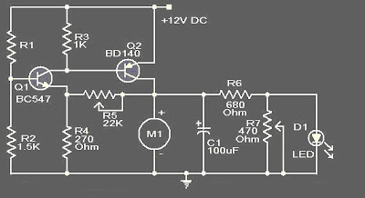
This circuit of automatic Control suhu is based on two transistors that can be used to control the speed of a 12 V DC fan depending on the temperature (suhu). A thermistor (R1) is used to sense the temperature. When the temperature increases the base current of Q1 (BC 547) increases which in turn decreases the collector voltage of the same transistor. Since the collector of Q1 is coupled to the base of Q2 (BD 140), the decrease in collector voltage of Q1 forward biases the Q2 more and so do the speed of the motor. Also, the brightness of the LED will be proportional to the speed of the motor.
Note:
  • R1 can be a 15K @ 20°C ,N.T.C thermistor.
  • M1: DC Fan 12V,700mA fan motor.
  • Capacitor C1 must be rated 25V.
  • The circuit can be powered from a 12V PP3 battery or 12V DC power supply.

About thermistor

The standard leaded thermistors are calibrated and tested at 20 °C to a tolerance of ± 5 % or ± 10 %; however, tighter tolerance, point matched thermistors are readily available as are special point match temperatures to fit your application. Since these thermistors have only one controlled point of reference (the point match temperature), the resistance at other
temperatures is given by the “Resistance vs. Temperature Conversion Tables” for the appropriate material curve. The resistance value at any temperature is the ratio factor times the resistance at 25 °C. The resistance vs. temperature conversion tables can
be found at: www.vishay.com/doc?33004 and www.vishay.com/doc?33011.